011
Layers
2 to 8, rigid only
Everything on this page is a number we build to. If your design sits outside one of them, ask — the answer comes from an engineer, not a sales script.
2 to 8, rigid only
FR-4 (Shengyi, Kingboard), CEM-3
0.075 mm (approx. 3 mil)
Up to 3 oz
ENIG, lead-free HASL, OSP, flash gold
0.2 mm
PTH ±0.075 mm · NPTH ±0.05 mm
0.4 to 3.2 mm
±0.05 mm
0.085 mm
Taiyo, RongDa, KuangShun
Lead-free and halogen-free builds available
IPC-A-600H Class 2
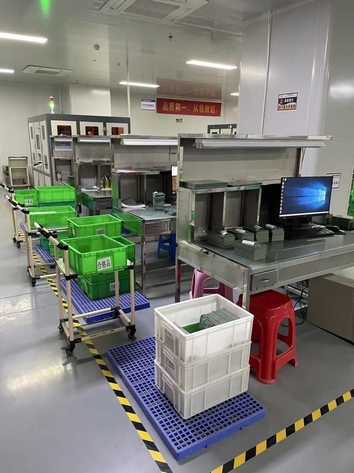
Electrical test, AOI and final visual inspection in the standard flow
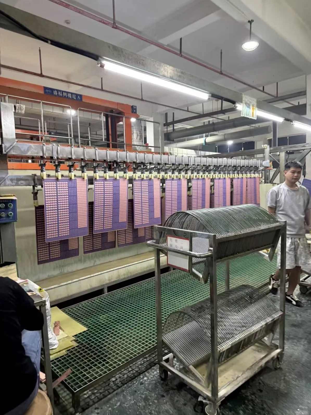
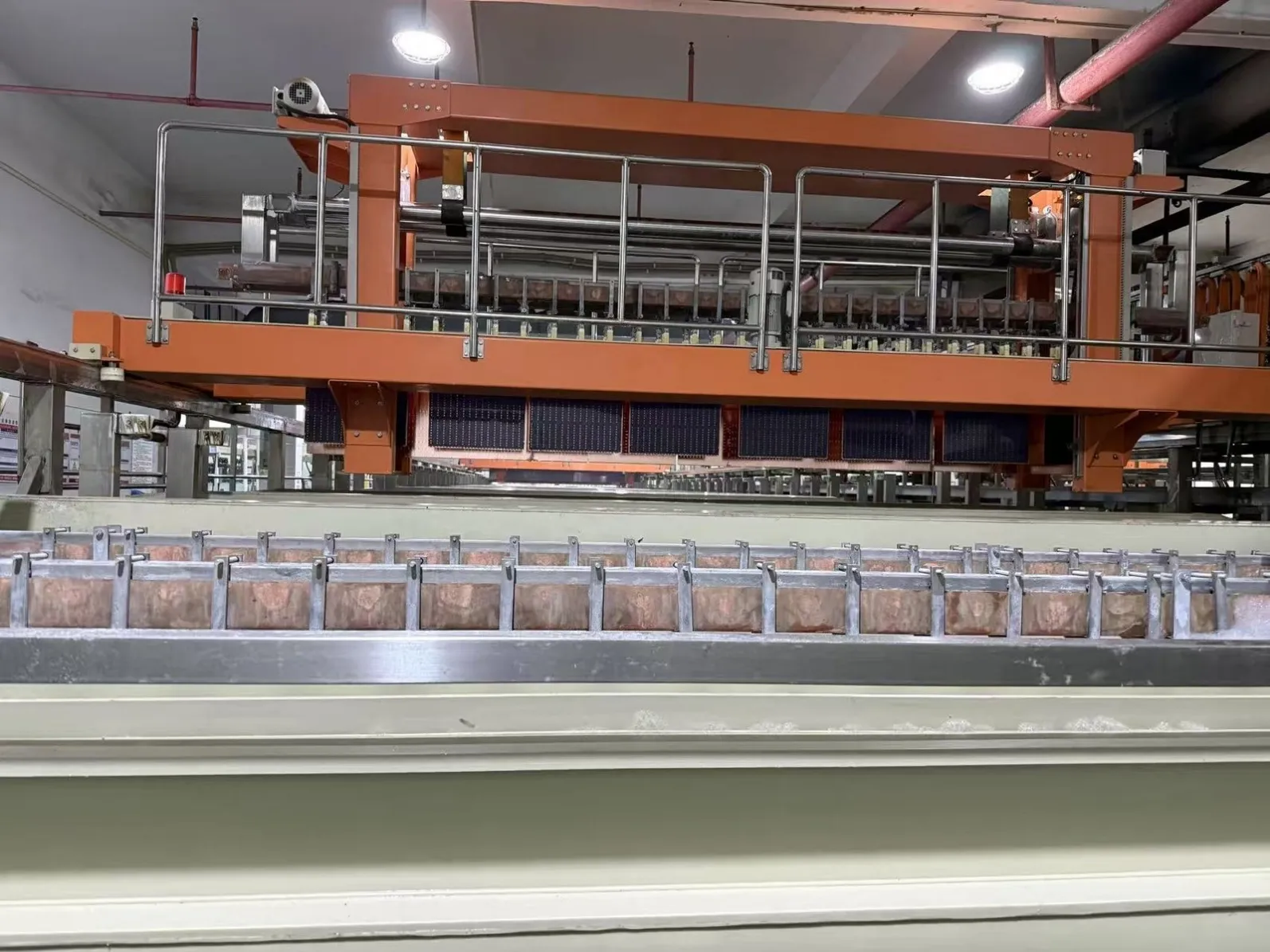
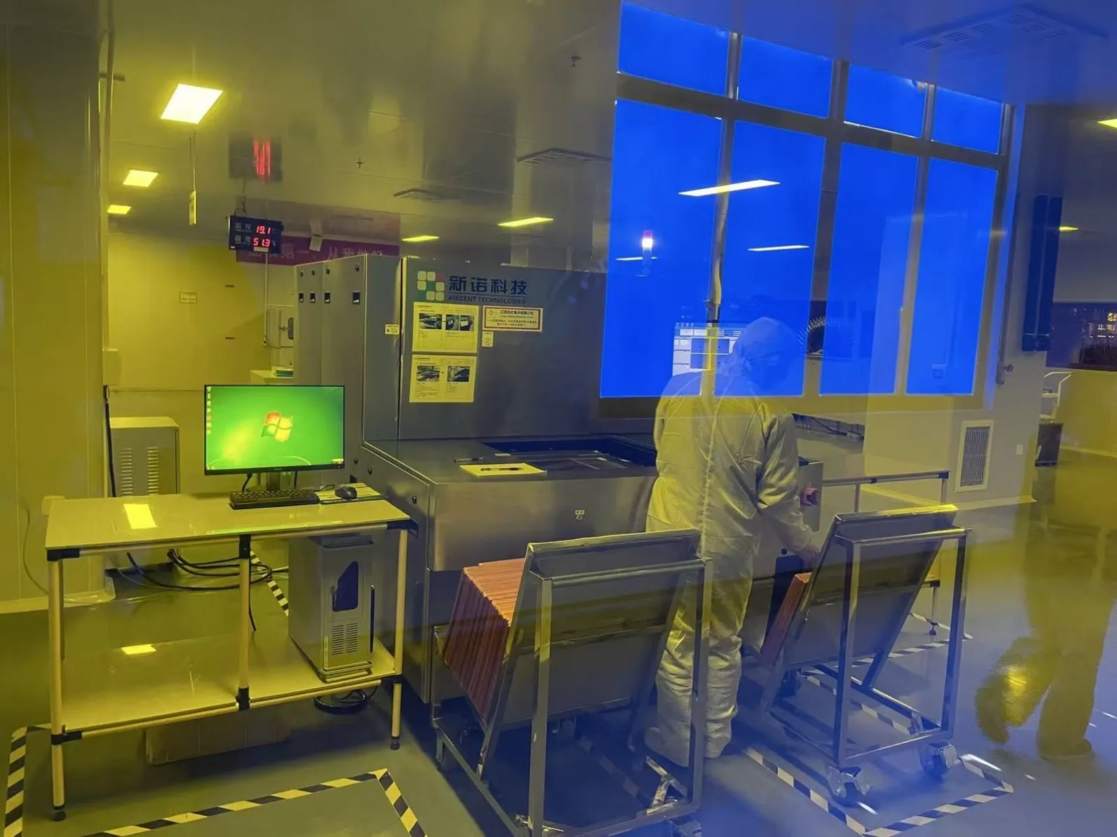
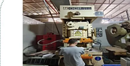
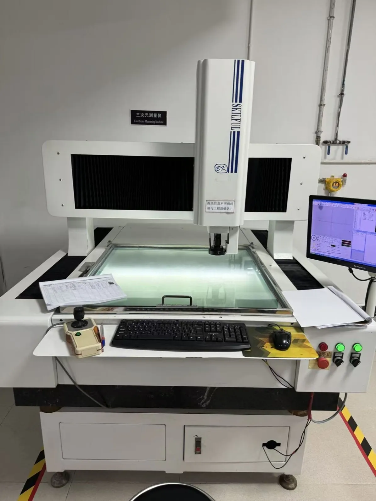
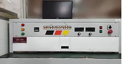
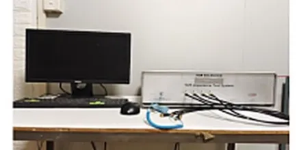
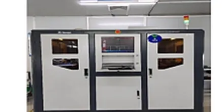
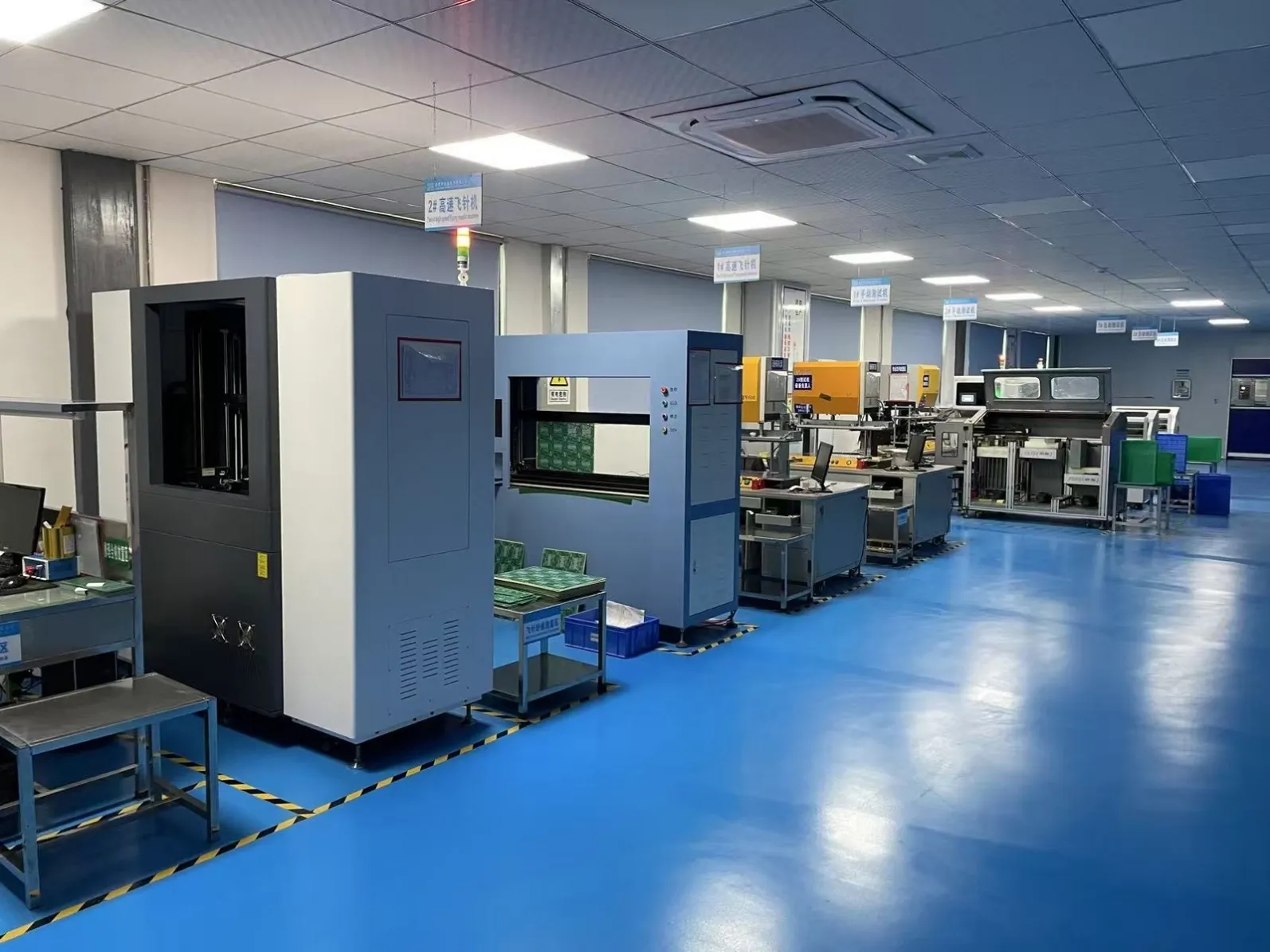
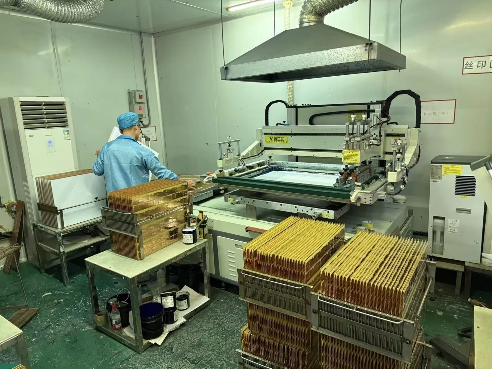
19 photos from the lines and test benches
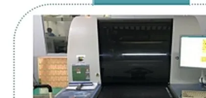
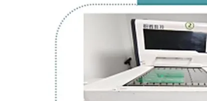
Every board is electrically tested and inspected before dispatch — flying-probe and automated testing, AOI and final visual inspection are part of the standard production flow.
Email your Gerber and drill files to midst_zhong@126.com with layers, thickness, copper, finish and quantity — or start with the form and just the basics. Free engineer DFM check with every quote.
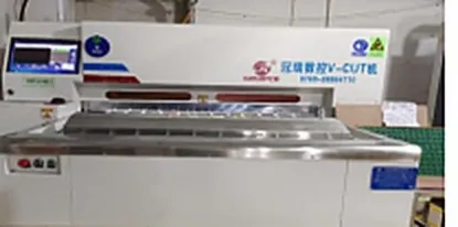
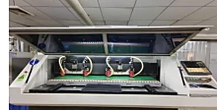
The lines and test benches your boards pass through — plating, imaging, profiling and electrical test are all in the standard flow.